Inside the ESP32: Architecture & Firmware Analysis
A deep-dive journey inside the ESP-WROOM-32 chip, exploring the Xtensa CPU, memory architecture, and how to reverse-engineer firmware to uncover its secrets.
The ESP32 Chip#
In the world of the Internet of Things (IoT), the name Espressif ESP32 has become extremely familiar. Recently, I got my hands on an ESP-WROOM-32 and started to wonder: What's really inside it? It's not just a simple microcontroller; it's a complete SoC (System-on-a-Chip) manufactured on a 40nm process.
On just one small chip, we have:
- Wi-Fi (2.4 GHz band)
- Bluetooth (Classic and BLE)
- Dual high-performance cores
- Ultra Low Power co-processor
- Multiple peripherals
In this article, we will explore this chip, from its unique instruction set architecture, how it manages memory, to "dumping" its firmware to see what it's hiding.
CPU: Why Xtensa and not ARM?#
The first curious thing is that the ESP32 doesn't use the popular ARM architecture (like in the STM32 or Raspberry Pi Pico). Instead, it uses the Tensilica Xtensa LX6 CPU.
Unlike the fixed instruction sets of ARM or x86, Xtensa is a customizable architecture. This demonstrates flexibility: Chip designers (like Espressif) can add custom instructions to the CPU to optimize for specific tasks, such as digital signal processing (DSP) or encryption, helping to accelerate hardware without needing a separate chip.
Symmetric Multiprocessing (SMP)#
The ESP32 is a dual-core system with two completely identical Xtensa LX6 CPUs. They share most of the memory and peripherals. This is a Symmetric Multiprocessing (SMP) architecture and is managed by FreeRTOS (a real-time operating system).
However, in practice, these two cores often have very clearly divided tasks:
- CORE 0 (PRO_CPU): Short for "Protocol CPU". This core typically runs protocol-heavy tasks like the Wi-Fi stack and Bluetooth stack. These network stacks are real-time systems; they must respond to packets within milliseconds. If they are delayed, the connection will drop.
- CORE 1 (APP_CPU): Short for "Application CPU". This is where the user's application code typically runs. This core is free to do anything (run a web server, read sensors,...) without fear of interfering with the Wi-Fi connection. 1
FreeRTOS is the manager that coordinates these two cores. It allows them to communicate safely with each other through mechanisms like Queues and Semaphores.
The ULP (Ultra-Low-Power) Coprocessor#
Besides the two LX6 cores, the ESP32 has a third brain: the ULP (Ultra-Low-Power) Coprocessor.
This is essentially a FSM (Finite State Machine) that can be programmed in assembly using the esp32ulp-assembler tool. The ULP operates in the RTC (Real-Time Clock) domain, allowing it to continue running even when the two main CPUs are in deep sleep mode.
The purpose of the ULP is to perform simple tasks like reading sensors, checking logic conditions, and waking up the main CPU when needed. It uses two separate memory regions:
- RTC_FAST_MEM (8 KB): contains the ULP's code (instructions).
- RTC_SLOW_MEM (8 KB): stores data and state, which is retained during deep sleep.
Thanks to this design, the ESP32 can perform periodic measurements or monitoring while maintaining extremely low power consumption—a crucial factor in battery-powered IoT applications.
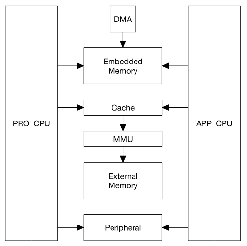
Memory Architecture#
The ESP32 is a dual-core system with two Xtensa LX6 CPUs following a Harvard Architecture, meaning it has separate buses for instructions and data.
All memory (embedded memory, external memory) and peripherals are located on the data bus and/or instruction bus of these CPUs.
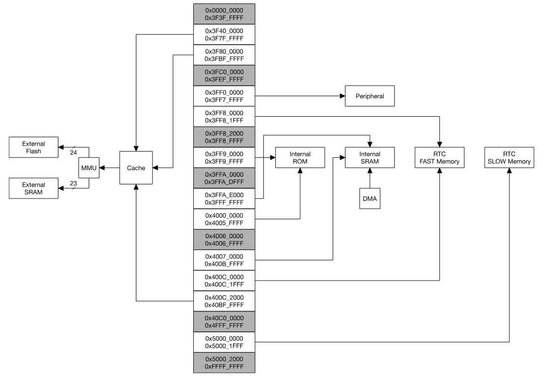
Address Space#
This is an extremely important and easily confusing point. The ESP32 has a 32-bit address space (4GB) for both the data bus and the instruction bus. This does not mean it has 4GB of RAM. It means the CPU can see 4 billion different addresses.
How the physical components are mapped into this 4GB space is up to the chip designer. On the ESP32, this 4GB space is divided as follows:
- 1296 KB for Embedded Memory
- 19704 KB for External Memory
- 512 KB for Peripherals
- 328 KB for DMA (Direct Memory Access)
Embedded Memory (On-Chip)#
This is the memory physically located inside the ESP32 chip; it is super fast.
- 448 KB Internal ROM: Very fast, but non-modifiable. It contains the First-Stage Bootloader (the first program that runs when the chip powers on) and core libraries (like some Wi-Fi functions, ROM processing).
- 520 KB Internal SRAM: Extremely fast. This is where code actually runs and data is stored. It is divided into IRAM (Instruction RAM, used to hold running code) and DRAM (Data RAM, used to hold data like variables, stack, heap).
- 8 KB RTC FAST Memory: Used for the ULP Coprocessor.
- 8 KB RTC SLOW Memory: Retains data even when the chip is in
deep sleepmode.
External Memory (Off-Chip)#
SPI memory (Off-Chip Flash) can be mapped into the available address space to be used as external memory. A part of the embedded memory can be used as a transparent cache for this external memory.
- Supports up to 16 MB off-Chip SPI Flash (this is where your application code is stored; my ESP-WROOM-32, for example, has 4MB).
- Supports up to 8 MB off-Chip SPI SRAM (less common, used for RAM expansion).
The block diagram in Figure 1 illustrates the system structure, and the block diagram in Figure 2 illustrates the address map structure.
The ESP32 only has about 520 KB of SRAM, but programs can be several MB large, residing on Flash. The solution is to use a part of SRAM as an instruction cache — allowing the CPU to execute code from Flash without loading the entire program into RAM.
The ESP32 uses a part of its Embedded Memory (SRAM) as a transparent cache for the external Flash memory.
When a CPU (e.g., APP_CPU) tries to execute an instruction at an address, the memory controller checks:
- Is this instruction in the cache (IRAM)?
- If yes: Execute immediately from IRAM (very fast).
- If no (Cache miss): The CPU pauses. The memory controller reads a block of instructions from SPI Flash (slow) and loads it into IRAM, overwriting an old block.
- The CPU resumes execution from IRAM.
This mechanism allows us to run programs much larger than the physical SRAM capacity. For specific address details, you should consult the ESP32 Technical Reference Manual—it lists all the register addresses.
Boot Process#
So, how do all these components (ROM, Flash, SRAM) work together? Everything starts when the chip is powered on:
- Stage 1 (ROM): The Xtensa CPU wakes up and starts executing code from a fixed address. This address points to the Internal ROM (448 KB). The program in this ROM (First-Stage Bootloader) cannot be changed.
- Check Boot Mode: The Stage 1 Bootloader reads the strapping pins to decide what to do next (e.g., boot from Flash or wait for a code upload command via UART).
- Stage 2 (Flash IRAM): In a normal boot, it loads the Second-Stage Bootloader from Flash memory (usually at address
0x1000) into IRAM (SRAM) and starts running it. - Read Partition Table: This Stage 2 Bootloader is smarter. It will find and read the Partition Table (usually at
0x8000) to understand the Flash layout—this is the same partition table we will analyze later. - Load Application: Finally, it finds the application partition (e.g.,
app0), uses the MMU and Cache mechanism we discussed to map this application into the address space, and transfers control to your code (thesetup()function begins).
This process clearly illustrates the relationship between ROM (used for booting), Flash (used for storage), and SRAM (used for execution).
Memory-Mapped I/O (MMIO)#
An interesting thing about microcontroller architecture is: the CPU (Xtensa) doesn't know what GPIO, UART, or SPI are. It only knows how to do two things: Calculate, and Read/Write Memory.
So how does it control an LED or read data from UART? The answer is Memory-Mapped I/O (MMIO).
A part of the 4GB address space is connected directly to the physical hardware of the peripherals.
- For example: The address space from
0x3FF44000is connected directly to the GPIO hardware. - The address space from
0x3FF40000is connected directly to the UART0 hardware.
When a programmer writes code like digitalWrite(LED_PIN, HIGH), the underlying library translates it into a command to write a value to a specific memory address (e.g., WRITE(0x3FF44008, 0x10)). The CPU just thinks it's writing to RAM, but the hardware intercepts this write command and changes the state of the GPIO pin.
This mechanism allows programmers to control everything (from Wi-Fi to I2C) using the same single mechanism: reading from and writing to specific memory addresses.
"Hello, Wi-Fi!"#
Next, let's run a simple "hello world" program to connect to Wi-Fi. I used PlatformIO to compile and upload the code quickly.
#include <Arduino.h>
#include <WiFi.h>

// Replace with your Wi-Fi credentials
const char *ssid = "YOUR-WIFI-NAME";
const char *password = "PASSWORD";

void setup()
{
  Serial.begin(115200);
  delay(1000);

  Serial.println("Starting WiFi...");
  WiFi.begin(ssid, password);

  // Wait for connection
  int attempts = 0;
  while (WiFi.status() != WL_CONNECTED)
  {
    delay(500);
    Serial.print(".");
    attempts++;

    if (attempts > 20)
    {
      Serial.println("\nFailed to connect to WiFi!");
      return;
    }
  }

  Serial.println("\nWiFi connected!");
  Serial.print("IP address: ");
  Serial.println(WiFi.localIP());
}

void loop()
{
  Serial.println("Logging data...");
  delay(2000);
}
After uploading the code, I opened the Serial Monitor and got this result:
Starting WiFi...
.....
WiFi connected!
IP address: 192.168.1.105
Logging data...
Logging data...
Great! It worked. I started to wonder where the ssid and password information is located in the chip now. Is it stored securely?
Reverse Engineering: What's inside the Flash?#
Next, let's perform Reverse Engineering (RE) to see what's inside that 4MB Flash memory.
Dump Flash#
I used esptool (a Python tool from Espressif themselves) to read the entire contents of the flash memory and save it to a file.
# Read 4MB (0x400000 bytes) from address 0x00000
esptool.py --chip esp32 --port /dev/ttyUSB0 read_flash 0x00000 0x400000 flash.bin
After a few minutes, I had a 4MB file named flash.bin.
Analyzing the Flash#
This flash.bin file contains everything: the bootloader, application code, and... possibly data too. I used another tool called esp32knife to analyze this dump file.
When running esp32knife, the first thing we find is the flash memory map, also known as the Partition Table. In my case, it was saved in parsed/partitions.csv:
# ESP-IDF Partition Table
# Name, Type, SubType, Offset, Size, Flags
nvs,data,nvs,0x9000,20K,
otadata,data,ota,0xe000,8K,
app0,app,ota_0,0x10000,1280K,
app1,app,ota_1,0x150000,1280K,
spiffs,data,spiffs,0x290000,1408K,
coredump,data,coredump,0x3f0000,64K,
We can see the main partitions:
- nvs (Non-Volatile Storage): Used to save key-value pairs, like Wi-Fi configuration info.
- app0/app1 (OTA): The ESP32 supports Over-The-Air updates.
app0is the main application (the one we just flashed),app1is where a new update would be stored. - spiffs: A simple file system for storing files (images, configs, web pages).
Searching for "Secrets"#
The interesting part is in the nvs (Non-Volatile Storage) partition. This is where the WiFi.begin() function stores the login credentials to automatically reconnect next time.
When checking the part.0.nvs.csv file (extracted by esp32knife), I found a surprise:
# Key, Type, Encoding, Value
...
wifi.ssid, data, string, "VEVOLVdJRklDVUFCQU4="
wifi.pwd, data, string, "TUFUS0hBVVdJRkk="
...
Those VEVOLV... and TUFUS... values look very familiar. They are my SSID and Password, encoded in Base64!
When I copied these strings and decoded them:
echo "VEVOLVdJRklDVUFCQU4=" | base64 -dYOUR-WIFI-NAMEecho "TUFUS0hBVVdJRkk=" | base64 -dPASSWORD
They are right there, stored as plain text (after decoding) right in the NVS partition.
Important Note: Base64 is not security encryption. It is just an encoding method, used by the NVS library to ensure that all data strings (even those with special characters) can be safely stored as ASCII text. As we can see, anyone with physical access to the chip can dump the flash and decode these strings easily.
If you want to protect data, you should enable the ESP32's Flash Encryption or Secure Boot features.
Conclusion#
The journey from a seemingly simple ESP-WROOM-32 chip has led us deep into its hardware architecture. We've seen that the ESP32 is not only powerful thanks to its two CPU cores, but also flexible thanks to the Xtensa architecture. We've understood the mechanism behind running 4MB of code on 520KB of SRAM (thanks to the cache), and how the CPU controls the outside world (thanks to MMIO).
Finally, by dumping the firmware, we saw that even sensitive information like Wi-Fi passwords can be extracted if not properly encrypted. The ESP32 is truly a complex and powerful system packed into a tiny chip.
views
— views
Nguyen Xuan Hoa
nguyenxuanhoakhtn@gmail.com